FDC610PZ
Description
This P-Channel MOSFET is produced using ON Semiconductor’s advanced PowerTrench® process that has been especially tailored to minimize the on-state resistance and yet maintain low gate charge for superior switching performance.
Key Features
- Max rDS(on) = 42mΩ at VGS = -10V, ID = -4.9A
- Max rDS(on) = 75mΩ at VGS = -4.5V, ID = -3.7A
- Low gate charge (17nC typical)
- High performance trench technology for extremely low rDS(on)
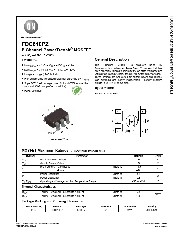
- SuperSOTTM -6 package: small footprint (72% smaller than standard SO-8) low profile (1mm thick)